Cheap and quick to produce, these digitally manufactured plasma sensors could help scientists predict the weather or study climate change.
Adam Zewe. MIT News Office
Publication Date:, July 27, 2022.

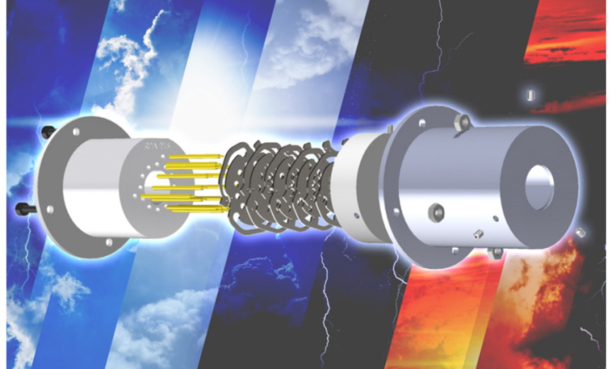
MIT scientists have created the first completely digitally manufactured plasma sensors for orbiting spacecraft. These plasma sensors, also known as retarding potential analyzers (RPAs), are used by satellites to determine the chemical composition and ion energy distribution of the atmosphere.
The 3D-printed and laser-cut hardware performed as well as state-of-the-art semiconductor plasma sensors that are manufactured in a cleanroom, which makes them expensive and requires weeks of intricate fabrication. By contrast, the 3D-printed sensors can be produced for tens of dollars in a matter of days.
Due to their low cost and speedy production, the sensors are ideal for CubeSats. These inexpensive, low-power, and lightweight satellites are often used for communication and environmental monitoring in Earth’s upper atmosphere.
The researchers developed RPAs using a glass-ceramic material that is more durable than traditional sensor materials like silicon and thin-film coatings. By using the glass-ceramic in a fabrication process that was developed for 3D printing with plastics, there were able to create sensors with complex shapes that can withstand the wide temperature swings a spacecraft would encounter in lower Earth orbit.
“Additive manufacturing can make a big difference in the future of space hardware. Some people think that when you 3D-print something, you have to concede less performance. But we’ve shown that is not always the case. Sometimes there is nothing to trade off,” says Luis Fernando Velásquez-García, a principal scientist in MIT’s Microsystems Technology Laboratories (MTL) and senior author of a paper presenting the plasma sensors.
Joining Velásquez-García on the paper are lead author and MTL postdoc Javier Izquierdo-Reyes; graduate student Zoey Bigelow; and postdoc Nicholas K. Lubinsky. The research is published in Additive Manufacturing.
Versatile sensors
An RPA was first used in a space mission in 1959. The sensors detect the energy in ions, or charged particles, that are floating in plasma, which is a superheated mix of molecules present in the Earth’s upper atmosphere. Aboard an orbiting spacecraft like a CubeSat, the versatile instruments measure energy and conduct chemical analyses that can help scientists predict the weather or monitor climate change.
The sensors contain a series of electrically charged meshes dotted with tiny holes. As plasma passes through the holes, electrons and other particles are stripped away until only ions remain.
These ions create an electric current that the sensor measures and analyzes.
Key to the success of an RPA is the housing structure that aligns the meshes. It must be electrically insulating while also able to withstand sudden, drastic swings in temperature. The researchers used a printable, glass-ceramic material that displays these properties, known as Vitrolite.
Pioneered in the early 20th century, Vitrolite was often used in colorful tiles that became a common sight in art deco buildings.
The durable material can also withstand temperatures as high as 800 degrees Celsius without breaking down, whereas polymers used in semiconductor RPAs start to melt at 400 degrees Celsius.
“When you make this sensor in the cleanroom, you don’t have the same degree of freedom to define materials and structures and how they interact together. What made this possible is the latest developments in additive manufacturing,” Velásquez-García says.
Rethinking fabrication
The 3D printing process for ceramics typically involves ceramic powder that is hit with a laser to fuse it into shapes, but this process often leaves the material coarse and creates weak points due to the high heat from the lasers.
Instead, the MIT researchers used vat polymerization, a process introduced decades ago for additive manufacturing with polymers or resins. With vat polymerization, a 3D structure is built one layer at a time by submerging it repeatedly into a vat of liquid material, in this case Vitrolite. Ultraviolet light is used to cure the material after each layer is added, and then the platform is submerged in the vat again. Each layer is only 100 microns thick (roughly the diameter of a human hair), enabling the creation of smooth, pore-free, complex ceramic shapes.
In digital manufacturing, objects described in a design file can be very intricate. This precision allowed the researchers to create laser-cut meshes with unique shapes so the holes lined up perfectly when they were set inside the RPA housing. This enables more ions to pass through, which leads to higher-resolution measurements.
Because the sensors were cheap to produce and could be fabricated so quickly, the team prototyped four unique designs.
While one design was especially effective at capturing and measuring a wide range of plasmas, like those a satellite would encounter in orbit, another was well-suited for sensing extremely dense and cold plasmas, which are typically only measurable using ultraprecise semiconductor devices.
This high precision could enable 3D-printed sensors for applications in fusion energy research or supersonic flight. The rapid prototyping process could even spur more innovation in satellite and spacecraft design, Velásquez-García adds.
“If you want to innovate, you need to be able to fail and afford the risk. Additive manufacturing is a very different way to make space hardware. I can make space hardware and if it fails, it doesn’t matter because I can make a new version very quickly and inexpensively, and really iterate on the design. It is an ideal sandbox for researchers,” he says.
While Velásquez-García is pleased with these sensors, in the future he wants to enhance the fabrication process. Reducing the thickness of layers or pixel size in glass-ceramic vat polymerization could create complex hardware that is even more precise. Moreover, fully additively manufacturing the sensors would make them compatible with in-space manufacturing. He also wants to explore the use of artificial intelligence to optimize sensor design for specific use cases, such as greatly reducing their mass while ensuring they remain structurally sound.
Reprinted with permission of MIT News (http://news.mit.edu/)

